Quantum Devices (QD) Department
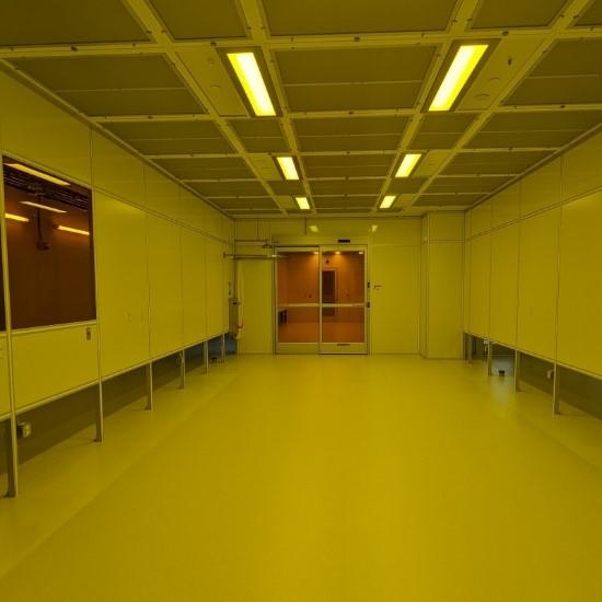
The Quantum Devices department performs R&D on superconducting quantum devices for computing, networking, and sensing. The breadth of our activities ranges from circuit design and fundamental materials studies to device packaging, cryogenic measurements and, with partners in the Advanced Instrumentation Division, full-stack integration with classical control and readout electronics. The centerpiece of our department is the Detector Microfabrication Facility (DMF), a vertically integrated class-100 superconducting device foundry that will launch in 2024.
Key Competencies
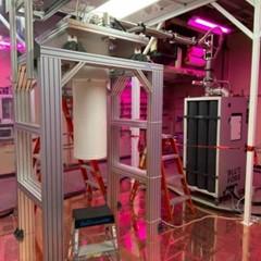
Cryogenic Device Measurement
Precision low-noise electronic testing of quantum devices down to mK temperatures. Cryostats range from rapid 4K test stands to dilution refrigerators, with a suite of DC, microwave, and millimeter-wave electronics for fabrication process testing and full quantum circuit measurement. Ex-DMF capabilities also include dicing and packaging facilities, shortening the time from fabrication thru device testing.
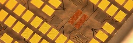
Superconducting Device Foundry
The DMF will begin operations in 2024 as a dedicated superconducting device foundry, the first of its kind in the DOE complex. A new 5,500 sq. ft. class-100 cleanroom has been constructed in the Arrillaga Science Center, and will house a complete tool suite capable of processing 150 mm-dia. wafers. Lithography tools include an ASML i-line stepper and Heidelberg direct laser-writer, plus electron beam lithography in the neighboring Nano-X cleanroom.